
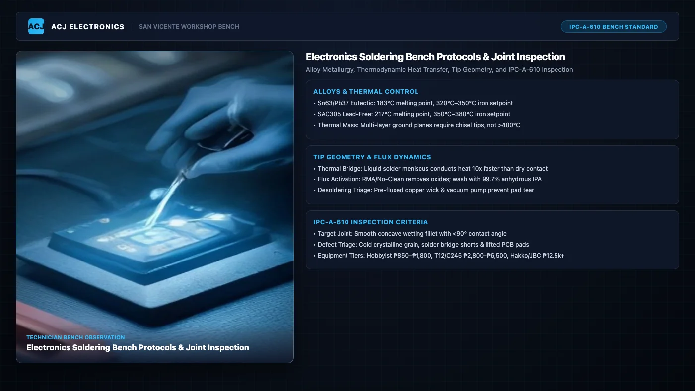
Electronics soldering forms an atomic-level intermetallic bond between copper pads and component leads by balancing thermal mass, activating oxide-clearing flux, and maintaining precise tip temperature. Controlled dwell time creates a smooth concave wetting fillet with contact angles below 90 degrees, preventing high-resistance cold joints, fractures, and lifted copper pads.
On my repair bench at ACJ Electronics in Poblacion, San Vicente, Ilocos Sur, the soldering station runs almost non-stop throughout the working day. From replacing cracked surface-mount charge ports on smartphones to reflowing high-current power transistors on audio amplifiers, soldering is not simple glue work. It is an exacting thermodynamic and metallurgical operation governed by physical laws.
Many beginners think that soldering is just melting shiny metal wire onto a circuit board until parts stick together. When repairs fail weeks later with mystery reboot loops, crackling audio, or torn traces, the fault almost always traces back to fundamental errors: using the wrong solder alloy, starving the joint of flux, picking a needle tip that cannot heat a ground plane, or cooking the circuit board at 450°C. Mastering real electronics repair requires understanding how solder wets at the molecular level, how heat travels through multi-layer copper, and how to inspect your work against professional engineering standards.
Core Soldering Physics and Metallurgy: Understanding the Bond
To produce joints that survive years of thermal expansion and mechanical vibration, a technician must look past the visible droplet of molten metal. True soldering creates an atomic-level metallurgical bridge.
The Eutectic Advantage: Sn63/Pb37 vs Lead-Free SAC305
When selecting solder for electronic circuit repair, the ratio of tin to other elements determines melting dynamics. In metallurgy, a eutectic alloy is a specific ratio of metals that melts and freezes at a single, sharp temperature point without passing through a slushy, semi-solid state.
Traditional Sn63/Pb37 solder is a true eutectic composition. At exactly 183°C, it transitions instantaneously between solid metal and free-flowing liquid. This zero-plastic-range property is invaluable on the repair bench. As soon as you remove the soldering iron, the joint solidifies cleanly in a fraction of a second. Even if a wire twitches slightly as the heat source pulls away, the joint will not crystallize into a fractured, high-resistance fault.
In contrast, modern commercial electronics use lead-free alloys such as SAC305 to comply with international environmental directives like RoHS. SAC305 melts at 217°C, which is a full 34°C higher than leaded solder. Because SAC305 has higher surface tension, it does not spread or wet copper pads as effortlessly as leaded solder. Furthermore, healthy SAC305 joints naturally exhibit a dull, satin, or slightly grainy surface rather than a mirror shine. Novice technicians frequently make the mistake of repeatedly reheating healthy lead-free joints because they expect a shiny leaded finish, ending up scorching the circuit board instead.
The Intermetallic Compound (IMC) Layer
Soldering does not work by sticking metal onto copper like hot glue. When molten tin contacts bare copper at soldering temperature, a chemical reaction occurs: tin atoms dissolve into the copper surface, forming a microscopic layer of copper-tin intermetallic compound (primarily Cu6Sn5 near the solder and Cu3Sn near the copper pad).
This IMC layer is the actual structural and electrical bond that holds the joint together. A healthy IMC layer measures between 0.5 µm and 1.5 µm thick. However, intermetallics are inherently brittle crystals. If you hold your soldering iron on a joint for too long (dwell time exceeding 4 to 5 seconds) or set your iron to 420°C, the IMC layer balloons to over 3.0 µm in thickness. When an intermetallic layer becomes that thick, any mechanical flex or thermal shock will shear the joint right at the boundary layer.
Thermodynamics and Temperature Control: Managing Thermal Mass
The single most destructive habit in electronics repair is cranking the station temperature knob to maximum whenever solder refuses to melt. Heat transfer is governed by thermal mass and contact surface area, not brute-force tip temperature.
Setting Iron Temperature Correctly
A properly calibrated soldering station should maintain an idle tip temperature approximately 120°C to 150°C above the liquidus melting point of the alloy you are using:
- Leaded Solder (Sn63/Pb37): Set the iron between 320°C and 350°C (608°F to 662°F). On single-sided boards with light traces, 320°C is plenty. For dense multi-layer boards, 340°C to 350°C provides adequate thermal headroom.
- Lead-Free Solder (SAC305): Set the iron between 350°C and 380°C (662°F to 716°F). A setpoint of 360°C is the sweet spot for general SMD rework.
- Absolute Hard Ceiling: Never exceed 390°C (734°F) on standard printed circuit boards. At temperatures above 400°C, the epoxy fiberglass resin (FR-4) that bonds the copper foil to the PCB core breaks down, resulting in blistered, delaminated, and lifted pads.
The Heat Sink Effect of Multi-Layer Ground Planes
Modern printed circuit boards in laptops, smartphones, and power supplies feature four to twelve internal copper layers. Solid ground and power planes are designed to distribute current and pull heat away from operating chips. However, when you attempt to solder a component pin tied to an internal ground plane, that copper plane acts as a massive thermal radiator, draining heat away from your iron tip faster than the heating element can supply it.
When this happens, novices reflexively crank their iron to 450°C. What happens next? The tiny tip still cannot supply enough energy, but the localized 450°C spike chars the surface solder mask and burns the flux away before it can activate. The correct solution is twofold:
- Switch to a wider tip with greater thermal mass: A 2.4 mm chisel tip stores far more thermal energy than a 0.5 mm needle tip and transfers wattage into the ground plane with minimal temperature drop.
- Use a preheater: On heavy multi-layer boards, placing the PCB on a magnetic bench preheater set to 100°C to 130°C elevates the baseline temperature of the entire board. Your iron only needs to provide the remaining 100°C to 150°C rise, allowing effortless joint flow without scorching anything.
Tip Geometry and Heat Transfer: The Solder Bridge Technique
Heat conducts through surface area contact. Air is an exceptionally poor conductor of thermal energy. Choosing the right tip shape and establishing a liquid contact bridge is what separates clean bench work from scorched frustration.
Selecting the Right Tip Profile
Using the wrong tip shape is like trying to loosen a lug nut with needle-nose pliers. Keep these four standard tip geometries on your bench:
- Chisel Tips (D-Series, 1.6 mm to 3.2 mm): The undisputed workhorse of electronics repair. The flat chisel face provides broad surface contact against both the component lead and the PCB pad simultaneously. Use chisel tips for through-hole pins, surface-mount passives (0805, 0603), power inductors, and ground lugs.
- Bevel / Hoof Tips (C-Series, 1.5 mm to 3.0 mm): Cut at a 45-degree angle with a flat circular or oval face. Many bevel tips feature a concave dimple that holds a small reservoir of molten solder. This is the premier tool for drag-soldering multi-pin surface-mount ICs like QFP and SOIC packages.
- Knife Tips (K-Series, 4.0 mm to 5.0 mm): Shaped like a miniature blade, allowing a technician to use the flat edge for broad multi-pin bridging cleanup or the sharp corner for tiny point repairs. Excellent for clearing solder bridges across fine-pitch SMD IC pins.
- Conical Needle Tips (I-Series / B-Series): Conical tips contact a flat pad at a single mathematical point, creating virtually zero thermal transfer area. Save needle tips exclusively for tight physical clearances, such as jumper wire work under a stereoscopic microscope. Never use conical tips on through-hole components or ground pins.
The Solder Bridge Technique: Instant Thermal Transfer
If you press a dry, freshly cleaned soldering iron tip against a cold component lead, almost no heat passes between them because microscopic surface roughness traps an insulating cushion of air. The technician pushes harder with the iron, which achieves nothing except flexing the PCB and risking mechanical trace delamination.
Instead, always use the solder bridge technique. Touch the iron tip against the workpiece, and instantly feed a tiny droplet (less than 0.5 mm) of solder wire directly into the junction where the tip meets the pad. That molten droplet forms a liquid meniscus (a liquid solder bridge) that conforms to both surfaces. Because liquid metal conducts heat hundreds of times faster than air, the entire joint reaches melting temperature in less than one second. Once the bridge forms, feed your primary solder wire into the opposite side of the joint to draw the alloy smoothly across the pad.
Flux Dynamics, Activation, and Residue Cleanup
Flux is not an optional additive. It is the chemical engine of soldering. Copper instantly develops a microscopic oxide layer when exposed to atmospheric oxygen, especially when heated. Molten solder cannot wet oxidized copper. Liquid solder simply balls up into a useless bead due to surface tension.
For a detailed breakdown of chemical formulations and bench safety, consult our guide on how to properly use flux in electronics repair. On the soldering bench, remember these key dynamics:
- Rosin Mildly Activated (RMA) Flux: Contains natural pine rosin fortified with mild organic activators. Activates between 130°C and 160°C to aggressively strip oxides. Its amber residue is relatively inert at room temperature, but should still be cleaned on high-impedance boards.
- No-Clean Flux: Formulated with synthetic resins and low-solids carboxylic acids. Leaves minimal, non-conductive residue. However, in high-humidity environments like the Philippines, unheated or partially activated No-Clean flux can absorb atmospheric moisture and create parasitic leakage paths.
- Water-Soluble (Organic Acid / OA) Flux: Highly aggressive halogen-based flux used for production. Highly corrosive. Any OA flux residue left unwashed on a circuit board will eat copper traces within weeks. Avoid OA flux for general bench repair unless you possess an industrial ultrasonic wash station.
Always clean finished solder joints with 99.7% anhydrous electronic-grade isopropyl alcohol (IPA) and an ESD-safe brush. Solvent cleaning removes ionic contaminants and flux residue that could cause microscopic dendritic growth or leakage currents on sensitive logic circuits.
IPC-A-610 Solder Joint Quality and Inspection Standards
In professional electronics manufacturing and repair, solder joints are judged against the strict visual acceptance criteria of IPC-A-610 (Acceptability of Electronic Assemblies). For consumer and industrial hardware, Class 2 (Dedicated Service Electronic Products) and Class 3 (High Performance / Critical Electronic Products) define reliability.
Target Acceptance Criteria
Under a stereoscopic microscope or 10x inspection loupe, a target-quality solder joint exhibits four clear visual signatures:
- Concave Wetting Fillet: The solder forms a smooth, inward-curving meniscus that tapers down to a feather edge on the copper pad. The contact angle (wetting angle) between the solder and the pad must be well under 90 degrees, ideally between 15 and 45 degrees.
- Visible Component Lead Contour: You should clearly see the outline of the wire lead or SMD terminal through the solder. A massive convex blob that hides the lead indicates excessive solder, which can conceal internal voids or cold bonding.
- 100% Barrel Fill on Plated Through-Holes: On multi-layer boards, solder must flow completely up through the vertical plated barrel to form a visible top-side wetting fillet, achieving at least 75% vertical barrel fill for Class 2 and 100% fill for Class 3.
- Clean Solder Mask Margin: Solder must remain fully confined to the exposed tinned pad without bridging onto adjacent copper traces or scorching the surrounding solder mask.
Identifying and Triaging Solder Joint Defects
When inspecting circuit boards for intermittent faults or verifying your own bench repairs, look for these specific defects:
Desoldering and Wick Cleanup Protocols: Protecting Fragile Copper Pads
Removing components cleanly is vastly more difficult than putting them on. When pulling through-hole components like DC power jacks, electrolytic capacitors, and multi-pin switches, the mechanical strength of the PCB copper pad is tested to its absolute limit.
Copper foil is glued to the fiberglass PCB substrate with a microscopic layer of cured epoxy. At room temperature, this bond is extremely strong. But when heated above 200°C, the adhesive softens dramatically. If you tug or pry on a component lead with pliers while heating the joint, the copper pad will tear away from the board like wet paper. Follow these three rules for damage-free desoldering:
- Pre-Flux Your Desoldering Braid: High-grade copper desoldering braid (wick) is woven from fine copper strands. While commercial wick comes treated with dry rosin, adding a drop of liquid RMA flux directly to the braid before touching the board dramatically accelerates capillary suction. The flux prevents the copper braid from oxidizing against the hot tip, drawing solder up into the braid in under two seconds.
- Zero Downward Mechanical Pressure: Place the fluxed braid over the solder fillet, rest the flat face of your chisel tip gently on top, and let thermal conductivity do the work. Never grind the iron tip down into the board. Grinding scrapes off the delicate solder mask and pushes the softened copper pad sideways, breaking its bond with the laminate.
- Lift Iron and Braid Simultaneously: As soon as the solder wicks into the braid, lift the iron tip and the copper braid away from the board together at the exact same moment. If you lift the iron first and leave the braid on the board for half a second, the remaining solder freezes instantly, soldering your copper braid securely to the PCB pad. Trying to yank a frozen braid off the board will tear the pad clean off. If the braid sticks, do not pull. Simply touch your iron back onto the braid, melt the solder, and slide it away smoothly.
For large through-hole joints, use a motorized vacuum desoldering gun (or manual spring-loaded desoldering pump) in combination with fresh solder. Adding a small amount of fresh leaded solder to an old, oxidized factory joint before pumping lowers the overall melting point and improves fluid suction through the plated barrel.
Soldering Station Buying and Equipment Recommendation Matrix
In our workshop at Poblacion, San Vicente, I have tested everything from cheap 60W plug-in irons to industrial cartridge stations. Investing in proper thermal recovery is the single best equipment upgrade any technician can make.
When starting out, avoid old-school passive 900M irons if your budget permits. A modern T12 or C245 cartridge system for ₱3,200 delivers ten times the thermal responsiveness, letting you solder multi-layer boards at 340°C that would choke a traditional iron set to 420°C.
Bench Case Study: Restoring an Audio Amplifier with Fractured Transistor Joints
To see how soldering physics directly impacts diagnostic triage and customer repair costs, look at a practical bench repair completed in our workshop at Poblacion, San Vicente.
Bench Repair Record: Intermittent Crackle on 150W Active PA Amplifier
- Client & Unit: Local events coordinator from Vigan City; 150-watt active stage monitor amplifier.
- Customer Reported Symptom: Audio cut out abruptly whenever bass hit hard; tapping the side of the wooden cabinet restored sound temporarily before crackling returned.
- Previous Assessment: Another shop suggested replacing the entire mainboard assembly for ₱4,200.
Diagnostic Isolation:
I placed the amplifier mainboard under my stereoscopic bench microscope. Tracing the power output stage, I inspected the solder joints connecting the two TO-220 packaged complementary output transistors (2SC5200 and 2SA1943) to the thick single-sided phenolic PCB.
Under 15x optical magnification, the failure was obvious: both collector and emitter pins showed severe ring-crack solder fatigue. The original factory solder was brittle lead-free alloy. Over three years of heavy usage, repetitive thermal cycling (transistors heating to 75°C under load and cooling to 28°C ambient) combined with continuous physical acoustic vibration from the adjacent 12-inch woofer had mechanically sheared the solder fillets. When bass thundered, the vibrating leads disconnected microscopically, causing instant audio cutouts.
Bench Reflow and Metallurgy Protocol:
- I coated all six transistor pins with rosin mildly activated (RMA) paste flux.
- Using a 2.4 mm chisel tip on my T12 station set to 340°C, I laid fluxed copper desoldering braid across each pin, completely evacuating the old, fatigued lead-free solder pool from both the top pads and through-hole barrels.
- I cleaned the scorched flux and oxidation off the copper rings using a nylon brush saturated with 99.7% anhydrous electronic-grade isopropyl alcohol (IPA).
- I applied fresh RMA gel flux and fed high-grade eutectic Sn63/Pb37 solder wire directly into the thermal bridge, creating shiny, concave, 360-degree wetting fillets with zero disturbance. The eutectic alloy provides superior flexibility and vibration damping compared to brittle lead-free solder.
Component Diagnostics and Integrated Bench Skills
Soldering is the hands-on execution phase of a complete diagnostic workflow. Before you touch an iron to a board, you must know exactly which component has failed and why. Solder work without diagnostic isolation is just guessing.
To build a complete bench skillset, connect your soldering techniques with these foundational diagnostics:
- Component Identification: Verify component polarities, package codes, and pin-one orientations using our guide to identify and replace common electronic components before desoldering.
- Circuit Schematics: Trace voltage rails and signal nets to confirm whether a suspect joint connects to ground or a sensitive data line by reading how to read electronics schematics.
- Multimeter Verification: Test diode mode drops and confirm zero continuity shorts across adjacent IC pins after soldering using our manual on how to use a multimeter for electronics repair.
- Core Diagnostic Protocol: Follow our master electronics troubleshooting guide to isolate hardware failures step by step.
- Tools and Skills Foundation: Explore our complete resource directory on the Tools and Skills Hub.
For complex logic board repairs or microscopic surface-mount component replacements in Ilocos Sur, you can consult our repair feasibility framework on the Repair vs Replace Hub or bring your device directly to our workshop in Poblacion, San Vicente.